All marketplace figuresFigure marketplace
Browse community-made TikZ diagrams and circuit examples. Edit figures on a visual canvas in TikzMaker and export the LaTeX code.
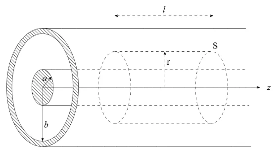
Coaxial cable drawn in perspective, with inner radius a, outer radius b, and a dashed cylindrical surface S of radius r and length l around the axis. The standard setup for applying Gauss's or Ampère's law to the field between the conductors.
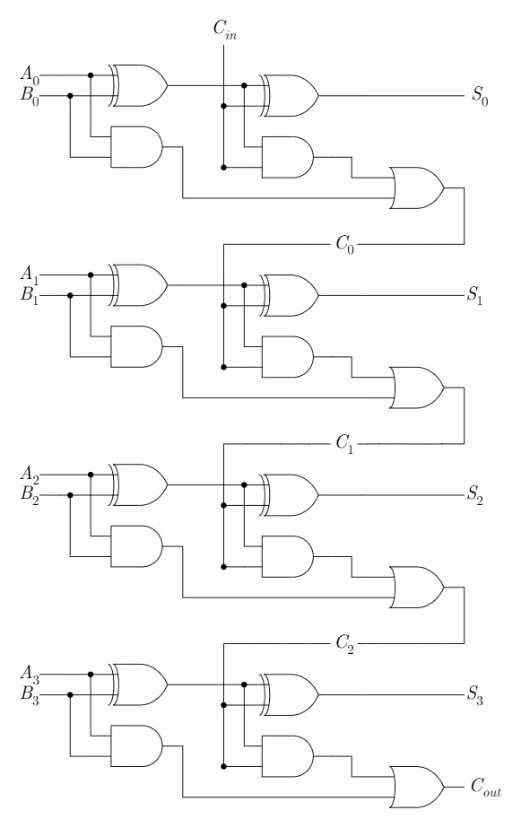
Gate-level implementation of a four-bit ripple-carry adder using cascaded full-adder stages. Each stage uses XOR, AND, and OR gates to compute the sum bit and carry, with each carry output feeding the next higher-order bit.
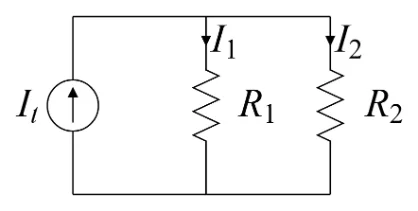
American-style current divider circuit with a current source feeding two parallel resistors, showing the branch currents \(I_1\) and \(I_2\) through \(R_1\) and \(R_2\).
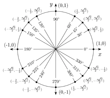
Unit circle showing common angles in degrees together with their exact Cartesian coordinates. The diagram includes the principal axes, standard special angles, and corresponding \((\cos\theta,\sin\theta)\) coordinate pairs.
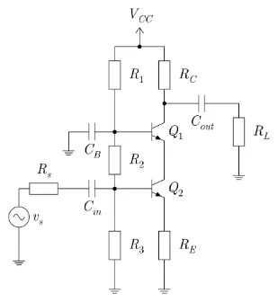
BJT cascode amplifier with a common-emitter transistor \(Q_2\) driving a common-base transistor \(Q_1\). The bias network \(R_1\), \(R_2\), and \(R_3\) establishes the operating points, \(C_B\) AC-grounds the base of \(Q_1\), and \(C_{\mathrm{in}}\) and \(C_{\mathrm{out}}\) provide input and output coupling. The output is delivered to load \(R_L\).
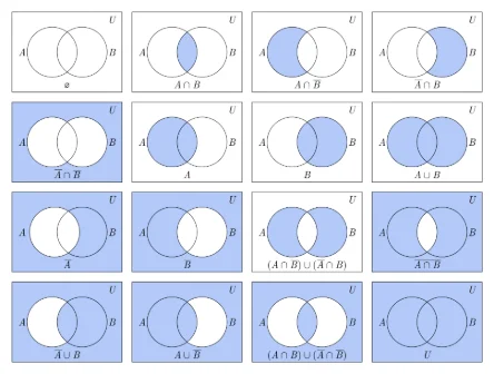
Reference chart of common set operations for two sets \(A\) and \(B\) within universal set \(U\). Shaded regions illustrate intersection, union, complements, set differences, symmetric difference, and related Boolean set expressions.
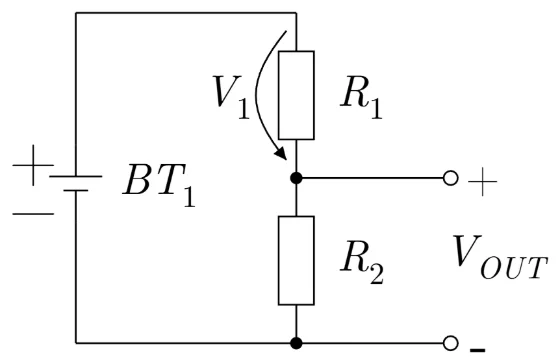
A battery BT1 across two series resistors R1 and R2, with the output taken from the junction between them.
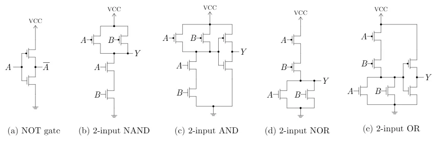
Transistor-level CMOS implementations of basic logic gates, including NOT, 2-input NAND, 2-input AND, 2-input NOR, and 2-input OR. The figure shows the complementary PMOS pull-up and NMOS pull-down networks used to realize each logic function.
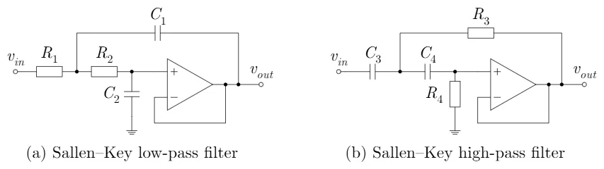
Comparison of unity-gain Sallen-Key second-order active filters. Circuit (a) shows the low-pass configuration using resistors \(R_1,R_2\) and capacitors \(C_1,C_2\), while circuit (b) shows the corresponding high-pass configuration using capacitors \(C_3,C_4\) and resistors \(R_3,R_4\).
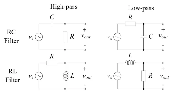
Comparison of first-order passive RC and RL filter circuits. The figure shows high-pass and low-pass configurations using resistors, capacitors, and inductors, with the output taken across the shunt component.
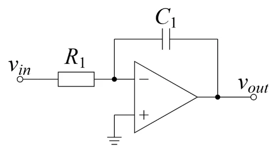
Ideal inverting integrator built from one resistor and one capacitor around an op-amp, with the non-inverting input grounded.
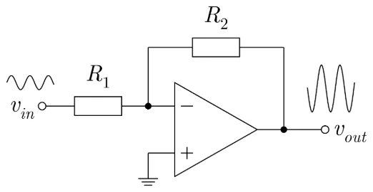
Inverting operational-amplifier circuit with input resistor \(R_1\) and feedback resistor \(R_2\). The non-inverting input is grounded, and the output is amplified and inverted relative to the input, with closed-loop gain \(A_v=-R_2/R_1\).